
- Samsung is working on rolling out the world's first 2nm process Exynos 2600 SoC on smartphones.
- The upcoming Snapdragon 8 Elite 2 SoC is itself based on 3nm process which pushes Samsung a step ahead with the 2nm process in the works.
- It is developing the chipset to reach 70% yield rate - the minimum to make the chipset viable for mass production.
Earlier on Friday, Samsung had its Q2 2025 earnings calls and announced the ramp-up production of Exynos 2600 SoC, its chipset made on a maiden 2nm process. This will definitely put Samsung ahead of its competitors like TSMC, which is sticking to the 3nm fab process, such as Qualcomm’s Snapdragon 8 Elite 2 SoC. Here’s what we know so far (and it is both exciting and skeptical).
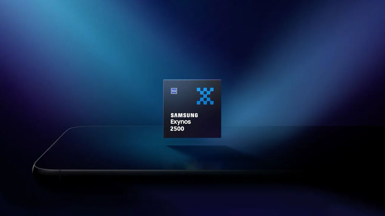
Samsung’s next-gen flagship phones (aka Galaxy S26 series) will be powered by Exynos 2600 SoC, the successor to Exynos 2500. Now that the obvious is out of the way, we wanted to tell you all that it will be the world’s first 2nm chipset available commercially on smartphones.
TSMC, which happens to rule the chip market, is currently Samsung’s biggest competitor, and it will come up with yet another path-breaking flagship chipset, aka Snapdragon 8 Elite2 SoC, fabbed on a 3nm chipset. This would make Samsung’s implementation of the new fabrication process the first of its kind.
The more we know about the 2nm Exynos 2600 SoC, the better it gets
Samsung’s Exynos 2600 SoC will be the South Korean giant to take a giant leap. It will be the first-ever 2nm chipset made by chipmakers, and Samsung Foundry (the arm behind the chipset) will become the first maker to roll it out.
Exynos 2600 is based on the Gates-All-Around (GAA) fabrication process, which is designed to control voltage and make it more efficient. Having a 2nm chipset compared to a 3nm node is better because the former unlocks more power, performance, and higher efficiency. For anyone you would ask, more power and efficiency are better. However, there’s a catch.
A few months ago, Samsung Foundry was tipped to have reached a yield rate of 30%. For context, if 100 wafers of silicon are prepared, a 30% yield rate means only 30/100 silicon wafers were successfully produced and can be reused; the rest is a loss, which is essentially transferred to the end users, raising the cost of the chipset.
Samsung vowed to touch a 70% yield rate – an ideal for chipmakers- by the end of this year, before it can commence minting Exynos 2600 SoC units on a large scale. With Samsung Galaxy S26 Series launch inching closer (ETA February 2026), the South Korean giant may not have much time to debut the chipset as well.

Samsung striked a $16.5 billion deal with Tesla
One of the points discussed at the earnings call was regarding the massive 16.5 bilion deal that the South Korean giant signed with Tesla for its 2nm chipsets. This should ultimately attract more customers, hiking the share price, and thus, minting more in ROI for Samsung. However, it all boils down to the yield rate and performance as well, which means there’s still a lot to cover.
Samsung is optimizing the Exynos 2600 SoC
Apparently, Samsung is still optimizing the Exynos 2600 SoC. It was recently spotted testing out Heat Pass Block (HPB) as a part of the Package-in-Package phase, allowing heat dissipation at the source. There were reports of the Exynos 2600 SoC appearing on Geekbench and other benchmarks so far. The chipset itself ought to get a 1+3+6 cores architecture with Eclipse 960 GPU (expected to be 15% more powerful than Adreno 830 GPU on SD8 Elite), to name a few.